F. Schmitt, A. Prieβner, B. Krämer and A. Gillner, Fraunhofer ILT
With new laser sources and integrated process control systems, optimized thermal management of the interconnection process can be provided, necessary for future thinner solar cells
The recent enormous growth of the photovoltaic solar cell industry has led to an increasing demand for flexible and efficient production technologies. For production rates of more than 1000 solar cells per hour, higher processing speeds are required, contributing to a further decrease of production costs. Laser processes have a high potential to meet these market and production driven demands for new solar cell concepts, generating a significant increase in efficiency and productivity for solar cell and module manufacturing.
Laser edge isolation is currently the only standard manufacturing for mono- and multicrystalline solar cells. However, there are at least a dozen processes under development and these will lead to new solar cell concepts with high efficiency and productivity. One of these processes is related to the interconnection of solar cells to solar modules.
Currently single solar cells with dimensions of up to 156 x 156mm² are interconnected by stringer tapes to large modules. Due to the decreasing thickness—less than 200μm—of silicon solar cells, contactless joining processes for module production are required to avoid increased scrap by breakage. A suitable technique for the electrical contacting of solar cells is non-contact laser beam soldering, because of the low and locally restricted energy input involved. By selecting suitable solders, the joining temperature can be reduced to a minimum and the solar cells are not subjected to mechanical stress, unlike when conventionally bow-type electrodes are used. A reliable soldering process can be demonstrated using a high-power diode laser system in combination with a highly dynamic galvanometer scanner and an integrated pyrometric process control system. Additionally, laser beam micro welding using a fiber laser could be used in future applications for special cell types, like emitter-wrap-through (EWT) and metal-wrap-through (MWT) cells with higher processing speed and lower thermal influence on the cell. In comparison to soldering, the process duration can be reduced by a factor of ten and the use of a fluxing agent can be avoided.
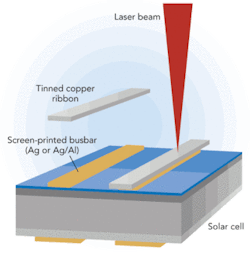
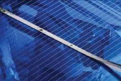
In solar module manufacturing, single solar cells have to be connected electrically to strings. Figure 1 shows the joining task in which a tinned copper ribbon has to be joined with screen-printed metallization, usually Ag or Ag/Al for cost reduction. This metallization is the so-called busbar, which collects the electrons generated in the solar cell and which is connected to the next cell in conventional solar module manufacturing by a thin stringer and hot air or IR lamp soldering systems using a bow type electrode.
Because the trend in silicon solar cell production is towards thinner thicknesses, below 180μm, the risk of cell breakage is increasing. Because the joining process is at the end of the entire value-added chain cell, breakage has to be reduced to a minimum. This has led to the demand for a contactless joining process with high reproducibility and controllability.
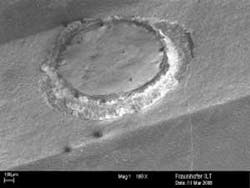
A conventional soldered joint after peel-test is shown in Figure 2. In SEM micrographs cracks in the basic silicon are visible. These cracks may lead to the failure of the entire solar module during a 25-year lifetime. Therefore, joining processes with a minimum thermal and mechanical stress induction are required.
Today, the main focus is on production technologies for standard screen printed frontside solar cells. New solar cell concepts like MWT or EWT will lead to a demand for more flexible production systems because of different solar cell designs from each solar cell manufacturer. Here, scanner-based laser systems offer the possibility for processing different solar cell designs with one system. This will enable the tool manufacturers to provide one system for different solar cell manufacturers. Moreover the new cell concepts require smaller and denser interconnections, which will require technologies with compact stringer feeding and a reduction of heating geometry for the cell interconnection.
Laser beam soldering
Laser beam soldering with its temporal and spatial selective energy input combined with the contactless operation is an attractive alternative to conventional soldering processes. The process was examined at the Fraunhofer ILT with diode laser systems with power to 250W in combination with fixed processing optics as well as galvanometric scanner systems for flexible joining geometries. The restricted use of certain hazardous substances in electrical and electronic equipment (RoHS) is limiting the use of lead for consumer products.1 This directive is not valid for solar module production, because there is no direct contact for the end user to the solar cell. For “green” products a green production technology without lead-containing solder alloys is required. Therefore the eutectic Sn63Pb37 is out of the question despite its good wetting, low melting point (183°C), and high reliability. Two alternatives are promising. The alloy Sn96Ag4 had comparable characteristics but the melting point is quite high (221°C). A second alternative is bismuth containing Bi58Sn42 with a melting point of 138°C.2
The soldering process was examined using diode lasers with low beam quality. The diode laser used has a maximum power of 250W, a focus diameter of 1.2mm, and a galvanometric scanner system is used to provide flexible joining geometries and process adapted thermal management. For the positioning and clamping of the contact stringer to the cell a contactless air pressure system is used to clamp both joining partners. If no clamping system is used, the heat dissemination into the solar cell is not sufficient due to non optimal contact and the copper ribbon is overheated. Because of the large working field, mechanical force has to be applied when a scanner system is used. A contactless clamping device for large working fields will be developed in the future.
For soldering applications a two-step process with an adapted temperature profile is recommended for high soldering qualities. In the first step both joining parts are heated up, so that wetting behavior will be increased and the fluxing agent activated. The temperature level of this first step is below the melting temperature of the solder alloy, as shown in Figure 3, left. In the second step, the laser power is increased, so that melting temperature of the solder alloy is achieved. A specific dwell time is necessary because the diffusion and wetting processes require a certain time. With pyrometers, developed at the Fraunhofer ILT for soldering applications, integrated coaxially into the optics system this two-stage profile can be monitored on line with respect to the resulting temperature. Furthermore, the whole process can be controlled by setting the laser power according to the measured temperature. The right side of Figure 3 shows the temperature signal (purple), nominal laser current (green) and reflected laser power (yellow) measured by a photodiode.
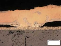
The analysis of the laser solder joints shows no damages to the silicon wafer and no cracks beneath the contact. For Sn96Ag4-plated copper ribbons (Figure 4, left) the soldered area can be detected. This area has dimensions of about 2 x 2mm2 with a thickness of solder layer of about 15μm. Using additional solder material like Bi58Sn42, the thickness of the interconnection is increased to 115μm (Figure 4, right). Peel forces between 3–4N are measured, comparable to conventional solder joints but with shorter joining times and less energy.
For laser soldering in production systems three different setups are possible: low-power direct diode lasers, high-power diode lasers with complex beam shaping, and high dynamic scanning systems with working fields up to 160 x 160mm2. In the latter, laser sources with a good beam quality are required due to the large working fields and the requirement of flexible adaptation of energy distribution in time and space. For a reliable production technology intelligent process control systems and algorithms have to be developed for fast scanning processes.
Laser beam welding
Laser beam welding is a promising joining technology for photovoltaic module production as an alternative to conventional soldering and laser beam soldering. Because of the high melting temperature of the copper ribbon, process thermal management and the avoidance of overheating, it is difficult to avoid damages to the crystalline silicon. Nevertheless, welding is a very interesting technology for future solar cells with respect to flexibility and quality because it does not require a fluxing agent. Thus the corrosive characteristics of these fluxing agents over the lifetime of the modules could be decreased. Nevertheless, a detailed examination on the negative impact of fluxing agents in solar module manufacturing is still unknown. A promising point is that processing times can be reduced to some 10ms compared to 100ms for soldering for each joint. Figure 5 shows a welded stringer for interconnection of poly-crystalline solar cells welded with the SHADOW micro ring process (micro ring with a diameter of 700μm).
null
null
The validation of the welding process for solar cells has been performed using conventional lamp-pumped Nd:YAG lasers and diode-pumped fiber lasers. The best results with minimum damage of crystalline silicon and a maximum peel forces can be achieved with a fiber laser power of 140W and about 50ms process duration shown in Figure 6. Damage of crystalline silicon cannot be detected and peel forces reach values up to 5N, which is within the specifications of a conventional solder interconnection joint. After peeling off the ribbons, the stringer remains partly on the silver based metallization of the solar cell as shown in Figure 7. Laser beam welding is at the cutting edge for the use in solar cell interconnection. Its feasibility can be shown but reproducibility is still restricted.
Conclusions
Laser processes provide many advantages in the manufacturing of solar cells. This holds for the processing of the silicon cells as well as for the interconnection of the single cells to complete modules. Laser soldering and laser welding provide low-energy solutions for high-speed packaging with high yield and high quality. With new laser sources and integrated process control systems, an optimized thermal management of the interconnection process can be provided, which will be necessary for future thinner solar cells.
Dipl-Ing. F. Schmitt ([email protected]), A. Prieβner, B. Krämer, and Dr.-Ing. A. Gillner are with Fraunhofer ILT, Aachen, Germany.
References
- Directive 2002/95/EC of the European Parliament and of the Council on the Restriction of the Use of Certain Hazardous Substances in Electrical and Electronic Equipment (RoHS), L37/19-L37/23, 2003.
- G. Humpston, D.M. Jacobson, Principles of Soldering, ASM International, 2004.


