BENJAMIN MEHLMANN and JOSEF SEDLMAIR
Power electronics constantly present packaging technologies with new challenges to handle ever-larger currents. At the semiconductor level, the most important interconnection technology by far is wire bonding with aluminum-heavy wires in diameters up to 500μm, welded directly onto a bond pad of the semiconductor chip by an ultrasonic friction welding process. These wire bonds have a fuse current of up to 35A for a wire measuring 20mm in average length. For considerably higher currents found in today's power modules, several wires are bonded in parallel on the chip.
Wire bonding features enjoy major advantages: the bonds are highly reliable and have long lives; the process is very flexible because distances and positions of the bonds can be freely programmed and adapted; and it is a very cost-efficient process.
However, two drawbacks to wire bonding are that the bonding surfaces must be very clean, and the bond pads on chips or substrates must be held rigidly and stably. The thicker the bonding wire, the more ultrasonic energy must be employed, making it progressively more difficult to clamp the parts rigidly. The bond forces also must increase with thicker wires. Taken together, these factors set a practical limit to about 500μm-diameter wire, as thicker wires pose a danger to sensitive chip surfaces.
Nonetheless, larger connector cross-sections have been processed for a few years now using ultrasonic wire bonding. These are usually rectangular ribbons measuring 2mm wide and 0.2mm thick, replacing three 500μm-diameter wires. The main area of application is automotive electronics, especially in e-vehicles.
Wire bonding
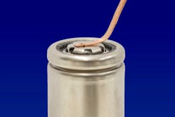
A further application has developed in the field of e-mobility for storage batteries. Depending on their design, they contain battery cells wired together by a variety of interconnection technologies. At present, the dominating battery type is the 18650 lithium-ion (Li-ion) consumer battery, which is especially well suited for wire bonding with heavy aluminum wire. Here, the advantages of the continuous bulk joint regarding lifetime and stability combine with excellent ease of automatization. This is the reason why wire bonding is by far the leading interconnection process for battery cells, for example, at Tesla Motors.
Even here, ultrasonic wire bonding is running into limitations of manageable currents. 18650 Li-ion-type consumer battery cells are operated with cells below about 20A, allowing a single wire to connect a cell to, for instance, a busbar. To connect several cells directly with a bond wire, however, the maximum current carrying capability is soon reached. Moreover, newer cells at the same approximate size are designed for currents up to 45A and would require several wires in parallel.
The alternative, using the aluminum ribbon mentioned earlier, is not really feasible: on the one hand, these ribbons are still quite expensive, and on the other it is difficult to clamp the cells well enough to sustain the higher ultrasonic energy input.
Laser welding
Laser welding is an alternative. In several regards, it is almost a perfect complement to wire bonding, as it has no trouble with lower-quality surfaces and it does not need substantial forces to clamp the parts during the process. Also, the connector elements can have large cross-sections to conduct very large currents. Finally, the requirements on the bulk properties of the connectors are lower, leading to lower material cost.
As with wire bonding, there are also a few disadvantages—notably the more difficult automatization compared to wire bonding. In wire bonding, the connector (wire or ribbon) is reeled from a spool in a virtually endless manner; is handled solely by the bonder; can be attached in any position and direction (also with tolerance compensation by pattern recognition systems); and can be cut at any length as needed.
Laser welding is more complex—a pre-fabricated connecting element must be positioned on the contact points and held there for welding. Therefore, the connector must be handled as a separate part and needs to be precisely positioned before the laser beam can start working. Furthermore, the connector must be pre-fabricated to the right dimensions, usually as a punched part. Tolerances and height variations in the contact positions cause extra work during process automation.
Laser bonding
Combining laser welding and wire bonding offers the best of both worlds, and it has now been accomplished within a joint research project supported by the German Federal Ministry for Education and Research (BMBF) called RoBE (Robustness for bonds in e-vehicles). Besides F&K Delvotec Bondtechnik (Munich, Germany) and the Fraunhofer Institute for Laser Technology (ILT; Aachen, Germany), the consortium included Audi, Continental, Infineon, and the Fraunhofer Institute for Reliability and Microintegration (IZM; Berlin, Germany).
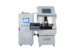
Developed within the RoBE project is the LaserBonder system, which consists of two main components: a standard wire bonder base from F&K Delvotec and a near-infrared fiber laser with 1kW power in a separate unit (FIGURE 1). The laser beam is brought into the bond head through an optical fiber, and ends up in a galvanometer scanner that contains optics generating a very sharp focus of about 35μm in diameter. The optics move the focused laser beam on the bond ribbon, just in front of the bond tool.
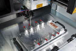
This bond tool is a modified type of bond wedge from ultrasonic bonding. Its main purpose is to hold down the bond ribbon properly on the contact pad. The rest of the bond head is unchanged from the ultrasonic bonder, including the wire or ribbon guide and the cutting unit, which indents the ribbon after the second weld step prior to tearing it off (FIGURE 2).Aluminum and copper connectors
Ribbon-shaped connectors are preferred over wires for laser bonding. Thanks to their rectangular cross-section, they feature a constant profile and, therefore, constant thickness of metal.
Aluminum is easily processed, as is copper. The latter is preferred on battery cells because of its higher conductivity. The bonder setup used is still largely restricted to the ribbon dimensions also used in the ultrasonic bonder—approximately 2mm wide and up to 0.3mm thick. Larger ribbons don't present a challenge for laser welding, but they do require a different layout for feeding and cutting, both of which are under development now.
In general, copper is considered much harder to process by laser welding than aluminum because at 1μm wavelength, it has poor absorption. One alternative is a green laser, which has much better absorption, but a much higher investment cost.
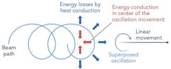
At Fraunhofer ILT, a technology was used that takes advantage of a very small focus spot. The extremely high energy density at this local spot permits deep-penetration welding instead of heat conduction welding, generating very deep and steep welding zones by internal multiple reflections. It is also termed keyhole welding because of this behavior. The side effect of a small connection area would normally be a narrow welding seam and, therefore, an undesirably high transition resistance. However, this is easily avoided by "wobbling" the laser beam, superimposed on the linear motion across the ribbon.
An additional advantage is that the heat emerging from the laser spot is not just dissipated on both sides of the welding seam, but is used efficiently to melt the area inside the circular movement (FIGURE 3). The result is a weld seam in which welding depth and seam width can be controlled independently, and that delivers consistently shallow welding depths into the lower contact pad.High current capacity/low weld penetration
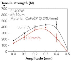
FIGURES 4 and 5 demonstrate how the mechanical strength of the weld seam and its width can be controlled by the advance speed and oscillation amplitude of the laser beam. Under optimized conditions, they can be more than doubled without increasing the process time and, therefore, the energy input. This is also attractive because the metallurgical properties of the welding zone depend strongly on the thermal load to which it is exposed.This is an aspect where laser bonding is highly advantageous, as it can make the connection on top of the rolled rim of the cell, right next to the plus pole. Having both connections on the top side of the cell leaves the entire remainder of the cell free of connecting leads, enabling simpler manufacturing because there is no need to flip the battery assembly, and far more space available for thermal management of the cell to help increase cell lifetime.
Different approach for larger currents
Larger prismatic battery cells where much larger currents are employed and where there are dedicated connector blocks on the battery cell require even larger ribbons. First steps are under development for ribbons up to 10mm wide and 1mm thick within the framework of FlexJoin, a joint research project funded by the Federal Ministry of Economy and Energy (BMWi).
An alternative to this is using pre-punched connector elements as in conventional laser welding. However, in the LaserBonder, only a different bond tool is needed and the bond ribbon is simply left out. The main advantage of the equipment is that it can push the connector element down to the contact block, ensuring a zero welding gap and making the clamping setup much simpler.
Because of the programmable laser beam pattern, a welding interface of any shape within a window about 10mm in diameter can be formed, allowing large operating currents. The downward push force and required distance can be controlled and monitored, allowing additional process and parts control. For some application areas, it may also be attractive to have equipment that is capable of both processes with extremely simple changeover.
Other applications
There are several further potential applications beginning to take shape. The lower demands of laser bonding regarding surface quality make it possible to bond aluminum ribbons directly to die-cast aluminum housings, without prior surface preparation. This is perfect for ground connections between printed circuit boards (PCBs) and the outer shell of many automotive aggregates such as starters or generators, as these should be continuous bulk connections without any mechanical or corrosion vulnerabilities for a very long lifetime.
Those are difficult and expensive to accomplish at present because bolting or crimping typically suffer from slow corrosion or oxidation. Also, ultrasonic bonding requires local surface preparation by milling, which generates conductive aluminum dust and requires expensive dust removal. Relatively thin (1500 × 100μm) aluminum ribbons are perfectly sufficient for the small grounding currents required, and they can be laser-bonded easily on the untreated cast aluminum surface. The second bond is made directly on a copper landing area on the PCB. If the copper layer on the PCB is very thin, it can easily be reinforced by soldering an extra copper pad to this spot during the standard surface-mount device placing process, causing very little extra cost.
Long-term objective
The long-term goal of laser bonding, however, is bonding directly on semiconductors-for example, copper ribbons for high currents on high-temperature wide-bandgap semiconductors such as silicon carbide. The welding depth and thermal energy input are still too high, creating a high risk of damaging the semiconductor, even where thick copper buffer layers are provided.
A novel approach called laser impulse metal bonding (LIMBO) is under development at Fraunhofer ILT, which is designed to bond across a defined small gap between the two welding partners. This approach decreases the amount of heat impinging on the semiconductor surface to a fraction of the regular technology, and shows great promise for rapid progress in the next few years.
BENJAMIN MEHLMANN ([email protected]) oversees laser bonding applications and Dr. JOSEF SEDLMAIR handles technical marketing, both at F&K Delvotec Bondtechnik, Ottobrunn, Germany; www.fkdelvotec.com.
