
Lasers provide a flexible and robust means of materials processing. Because they deliver energy remotely and require no physical contact between the laser and the workpiece, new materials or workpiece geometries can often be addressed with only a straightforward adjustment of process parameters. In 2017, Nuburu (Centennial, CO) brought the first industrially relevant blue laser to market, enabling the power of laser processing copper, gold, aluminum, and other reflective metals. Less than three years later, the industrial blue laser has achieved another milestone: power and brightness are now high enough to weld copper when integrated with standard industrial scanning systems. These new capabilities open up the possibility to weld greater thicknesses of copper and other challenging materials, and also improve the ability to weld dissimilar metals.
The blue industrial laser
Traditional infrared (IR) industrial lasers are not well suited to processing copper and many other reflective metals because those materials absorb only a few percent of their incident laser energy. To initiate a weld in copper, for example, an IR laser must deliver 20X more energy than required to melt the material. Once the melt is initiated, however, copper absorbs more IR energy, which creates localized miniature “explosions” within the melted copper. Those explosions eject material from the melt, leaving behind holes—known respectively as spatter and voids.
Spatter and voids reduce both the mechanical reliability and electrical fidelity of the welded joint. Various laser beam exposure patterns, known as “wobbling,” can reduce these problems, but not eliminate them. Also, there are some geometries for which no combination of exposure time and energy can produce a weld.
Blue lasers change the game. As shown in FIGURE 1, copper absorbs blue light more than 13X better than it absorbs IR. In addition, absorption doesn’t change much when the copper melts. Once a blue laser initiates a weld, the same energy density will keep that weld going. The process is inherently well controlled and error-free, and the result is the fastest, highest-quality copper weld possible.
Color and energy density
The advantage stems from fundamental physics: copper absorbs blue light better than it absorbs IR, and 20% better than it absorbs green light. That’s the start of the story, but it’s not the end. The energy density delivered to a workpiece must match the energy density needed to achieve a given aim. Continuing with the example of welding—more taxing than etching or cutting—the aim is to melt the target material. That takes about 2.3 MW/cm2; higher than that results in spatter and voids, while a density much lower will result in lower penetration depth and slower welding speeds. Precise process control enables the energy density to be set as high as possible and still maintain defect-free welding.
The energy density delivered to a surface depends on the power of the source, the exposure time, and the size of the spot at the workpiece. Although attention is given to laser power, the spot size at the surface is even more important. For example, if two blue lasers each put out 500 W, but Laser One delivers it in a 400-µm-diameter spot and Laser Two produces a 200 µm spot, Laser Two will have 4X the power density. This translates directly into performance advantages. As schematically illustrated in FIGURE 2, Laser Two penetrates more than 1.5X as deep into copper or welds the same thickness 3–4X faster.
The spot size is a function of the beam parameter product (BPP). In the example above, Laser One has a BPP of 60 mm-mrad, while Laser Two’s BPP is 30 mm-mrad. That is, a smaller BPP results in a smaller spot size and a higher energy density. The BPP is a function of laser design and cannot be improved by modifying the beam downstream of the source. The best that can be done is to maintain the BPP through the optical train.
Getting brighter
Nuburu introduced the initial high-power 150 W AO blue laser in 2017 and a year later, a 500 W AO unit was brought to market. In 2019, the company released a 1.5 kW 450 nm AI laser with a BPP of 11 mm-mrad. These lasers have a unique “chip-based” design feature that allows the output of each gallium nitride (GaN) diode to be collimated individually. If the diodes were to be collimated collectively by a single lens, as in “bar-based” technology, the BPP would unavoidably increase. Collimating each diode with its own dedicated lens minimizes the BPP and also presents a natural path for upgraded laser power, as GaN diodes follow their anticipated development roadmap.
The high brightness of the 1.5 kW AI laser has reached a key performance milestone: it’s the first blue laser to be integrated with scanning systems. Scanning systems are used in several industries to maximize productivity. These systems use what’s called an f-theta lens to convert an input angle to an output position. That is, a change in input beam angle results in a position change at the output plane. Where a simple lens would introduce changes in spot symmetry, f-theta lenses minimize asymmetries, allowing consistent exposure across the working surface, typically a 100X 100 mm field at a working distance of 300 mm. F-theta lenses do, however, introduce beam divergence—they spread the beam out. To produce a 400 µm spot, the input laser needs to have a BPP of 12 mm-mrad or less. The 1.5 kW, 11 mm-mrad AI unit creates a 400 µm spot, which delivers the 2.3 MW/cm2 required for defect-free copper welding at maximum depth and speed.
Such scanning systems are used in battery fabrication, e-mobility production, and consumer electronics manufacturing. The laser output power and dwell time can be adjusted in the course of a scanning operation, maximizing productivity by allowing different joining geometries and material thicknesses to be addressed in a single scanning pattern.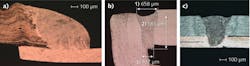
More power, more materials
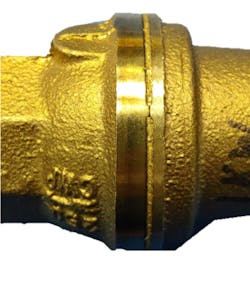
The AO series lasers are optimum for welding copper foil and busbars at thicknesses up to 500 µm—perfectly matched to the fabrication needs for certain battery types, such as cylindrical cells and some pouch cells. The higher power and brightness of the AI series allows greater thicknesses to be welded in a variety of materials: copper, gold, and stainless steel up to a few millimeters thick. It is ideal for manufacturing prismatic battery cells, fabricating cell casings (as shown in FIGURE 3), and battery pack and battery integration. The greater penetration depth also opens up e-mobility applications; as shown in FIGURE 4, the blue laser can produce hairpin welds that are important for dense and powerful electric motors. High power and brightness also add flexibility to the welding process, making it possible to extend the range of materials. For example, as seen in FIGURE 5, it’s now possible to weld brass, a common material in appliance production.
The future of blue
The brightness and power of blue lasers continues to push new boundaries. The increase in capability leads to an added range of applications as well. For example, the additive manufacturing capabilities of the blue laser are just being explored.
Cladding is an additive manufacturing application where one material is adhered to the surface of another. Typically, this is for environmental protection, although it also can improve thermal and electrical conductivity. The key is to produce a uniform, complete, defect-free layer covering the outside of a metal form, such as an Inconel cladding on steel wire. The same performance advantages that apply to blue laser welding also apply to blue laser cladding. Those physical advantages result in unmatched capabilities, such as the ability to coat stainless steel with copper, or even coat copper with copper.
Laser metal deposition (LMD) is similar to resin-based 3D printing. In LMD, however, the feed material consists of metallic powder. A powder stream is directed into the fabrication bed, and a laser melts the powder together in precise locations to create a final form of arbitrary shape. Again, the wide process window of the blue laser opens up the possibility to bring new materials and new efficiencies to LMD.
Blue laser technology has advanced rapidly, and the roadmap to multikilowatts is clear. If the past is any indication, it’s likely that the applications for blue laser processing will advance equally rapidly.