Ultrashort-pulse (USP) lasers deliver photons to the workpiece that are capable, if delivered correctly, of imparting little or no heat to the process. This is the major benefit of working in this pulse length regime. In the last 20 years, USP lasers have taken off as an industrial processing tool, focusing on cutting and drilling applications, especially those where the required end product could not be achieved with longer pulse-length lasers, or where significant and costly post-laser processing was required. Currently, a number of different surface application areas are being investigated and even used in production environments.
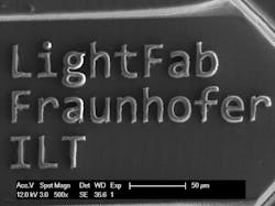
One important laser application area is additive manufacturing. USP lasers are not generally thought of as the laser to use for this process, since their virtue is no heat, but they are being investigated for direct laser-assisted deposition to produce precise or sensitive parts and they are also being used for precision post-processing of laser-assisted manufactured parts. For instance, it is possible to print 3D structures with acrylic resin using two-photon polymerization. Very fast writing speeds are possible using commercially available software. Figure 1 shows a part made with a 1.5 µm layer height and 2 µm resolution at a writing speed of 200 mm/s.
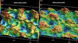
Marking, however, still accounts for most laser units sold. These lasers and systems tend to have low selling prices, so using a more-expensive USP laser in a marking application is only done in special circumstances. One such area is in marking stainless steel for medical devices. It happens that USP laser-marked parts are superior to those marked by any other method and it can even be used to make different-colored marks, depending on the laser conditions. Figure 2 shows a highly magnified image of the difference between a white and a black femtosecond mark on a stainless steel surface. The mark was generated using a feature called BiBurst, which combines megahertz and gigahertz bursts in the same job.Most of the USP laser activity is still in the area of material removal. For instance, a huge market area is being created for three-dimensional features on roller surfaces used in mold and die production. Another potentially large market area is in creating surfaces with certain hydrophilic (or hydrophobic) properties (see http://bit.ly/ILS-Femto). Such features are typically from a few microns to a few hundred microns in depth and are created by direct laser ablation. The process of creating these features is not complicated, even with a simple optical setup. However, the process of scaling things up to engrave rollers that are many feet long, and maybe also as wide, economically and precisely is key to integrating USP lasers into production environments.
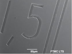
Glass is hard to laser-process with longer pulse-length lasers, but they can be either directly ablated with USP lasers or, for some materials, exposed and then chemically etched thereafter. Figure 3 shows a high-resolution micrograph of a femtosecond laser-ablated glass slide.Other possible uses of USP lasers on surfaces are cleaning or decontamination and polishing. For small surface structures, the best surface roughness that can be achieved with direct laser ablation is Sa = 0.5 µm. This is not sufficient for many applications and, therefore, a polishing process must follow the laser ablation. There is a benefit if the same USP laser and optical setup can be used for both steps and it has been shown that the process on metals involves producing a thin molten layer, which then distributes material more evenly on the surface. Resulting Ra <0.3 µm has been shown, and USP polishing on some polymers has shown a resulting Ra of <100 nm.
In order to scale up the process, it requires using either higher energy per pulse or pulse repetition rate. There is a limit in raising the pulse energy because too much will frequently overload the process with heat, thus negating the primary benefit of USP lasers. Beam splitting can be a solution to this problem; however, as USP lasers are normally capable of very high repetition rates (1–10 MHz or more), the usable repetition rate is limited if the beam cannot be moved fast enough to avoid dwell times long enough to impart heat to the material. Also, in order to fully use the available capability, the pulses must be triggered so that they are delivered uniformly, including during acceleration, which is especially true if using a USP laser. Therefore, the goal of covering large surfaces economically has been hard to achieve. Advances in technology now allow very fast delivery of high-repetition-rate USP light to large functional surfaces.
Many coordinated efforts (lasers/optics/systems/applications) are being done throughout the world to promote more industrial use of USP lasers on a large scale. For example, natural surfaces demonstrate how special nano- and micrometer-sized features can render surfaces superhydrophobic (such as a lotus leaf repelling water) or antibacterial. Laser-based texturing is a technique capable of imitating natural surfaces and functionalizing them without the use of additives. According to Dr. Lars Penning, Managing Partner of Next Scan Technology (Evergem, Belgium), the EU-funded project LAMpAS aims at achieving high throughputs with systems based on kilowatt-level USP. Enabling this technology will ensure that USP lasers play a role in the competitive manufacturing and commercialization of domestic appliances with new features, and other fast-moving consumer products.
The LAMpAS system will integrate a picosecond laser based on thin-disk technology, delivering up to 1.5 kW at a megahertz-level repetition rate. The laser-based machine will allow both high resolutions (feature sizes from 200 nm to 200 μm) and high throughput (up to 1–5 m2/min) to address both the functionality and the commercialization purposes.
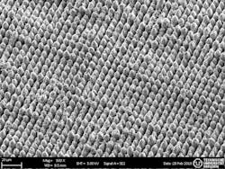
Applying nano- and micrometer-sized features is achievable, thanks to a multibeam processing technique with interference patterns called direct laser interference patterning (DLIP). This technology enables production of repetitive surface structures based on the local ablation that takes place at the intensity maxima position of the interference patterns. In case of the LAMpAS project, the interference patterns are produced by overlapping two laser beams in combination with a polygon scanner system. An example of a pillar-like structure produced on aluminum surface is shown in Figure 4.Furthermore, with an in-line monitoring system for process control, controlling the interaction between laser light and the substrate, these technologies can also stimulate self-organization processes generating laser-induced periodic surface structures (LIPSS) in a homogeneous way at a micrometer and sub-micrometer scale. The combination of structures with different feature sizes is relevant for reaching enhanced surface properties. This approach will result in applying many other unique surface properties. The LAMpAS project has received funding from the European Union’s Horizon 2020 research and innovation program under grant agreement No 825132. It is an initiative of the Photonics Public Private Partnership (photonics21.org).
Just a few years ago, I used to keep track of all USP laser manufacturers and their available products, but the laser field has grown so much in the last few years that I no longer do this. The laser manufacturers are all working to make their lasers more reliable, lower cost, and easier to integrate with other components in order to achieve the end product on a large scale, which is needed to fully implement USP lasers into industrial environments. It seems things are headed in the right direction and well on their way.


