Due to their small diameter and high flexibility, fiber-optic microendoscopes enable valuable biomedical procedures such as in vivo neural imaging, minimally invasive diagnostics, and microsurgery. In these single-fiber microendoscopes, laser light is passed down through the fiber to the tissue being examined; fluorescence emitted at the spot, which is scanned across the tissue, is collected by the fiber and enables the construction of a tissue image.
The microendoscope’s optical fiber requires an imaging lens at the probe end to maximize resolution. Commonly, a gradient-index (GRIN) lens is used, but such a lens is bulky in relation to the fiber and also, at best, produces a focal spot twice as large as the diffraction limit. Methods have been developed to produce a microlens at the tip of the fiber, such as forming via glass-pulling or melting and resolidifying the fiber end using a plasma discharge. But such lenses cannot be formed optimally, and thus are restricted to low numerical apertures (NAs).
But two-photon direct laser writing, which can be used to create micro-optics and other components, is now being exploited by researchers from RMIT University (Melbourne, Australia) and the University of Shanghai for Science and Technology (Shanghai, China) to write high-quality aspherical microlenses directly onto the tip of the microendoscope fiber; the lenses are aberration-free and high-NA, producing a spot down to 0.85 μm in size.1 (Because the light that is focused to form a spot is monochromatic, chromatic aberrations are not a concern; the lenses also collect the resulting fluorescence light, but light collection doesn’t require extremely high imaging quality.)
The fiber in the experimental device has a 40-μm-diameter core, 125-μm-diameter cladding, and a cladding-stripped end length of 84 μm. The laser-written lens is made of photoresist from Nanoscribe (Karlsruhe, Germany), a well-known supplier of supplies and systems for making microcomponents via two-photon processes. Aspheres with NAs of 0.3, 0.6, and 0.9 were designed in Zemax (Kirkland, WA) lens-design software for an operating wavelength of 590 nm; when operating monochromatically at laser wavelengths of 561, 590, or 630 nm, the designs are all diffraction-limited.
Lens fabrication
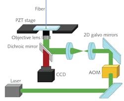
To write the lenses, light from a femtosecond laser at a 535 nm wavelength, 270 fs pulse duration, and repetition rate of 50 MHz was sent through an acousto-optical modulator (AOM) and a galvo scanner and focused by a 1.4 NA 100X microscope objective into the photoresist (see figure); the fiber was mounted onto a piezoelectric (PZT) stage and moved to provide one scanning axis (the galvo provided the other). The resist was then developed, with no further baking, polishing, or other operations required.
To characterize the point-spread functions (PSFs) of the lenses, light at 561 nm was sent through the fiber and the resulting focused spot examined with a 40X 0.65 NA objective; a Gaussian was fit to the resulting spot cross-section. The measured full-width at half maximum (FWHM) of the spots produced by the aspherical microlenses with NAs of 0.3, 0.6, and 0.9 were 2.00, 1.23, and 0.96 μm respectively; deconvolving the PSF of the microscope objective resulted in spot sizes of 1.95, 1.15, and 0.85 μm, respectively.
The researchers fabricated a test fluorescence sample on glass using Rhodamine 5G dye vie two-photon direct laser writing, then generated images from the fiber-optic probe with good results (in this test, the sample itself was scanned; for practical use, a microscanner could be added to the fiber probe).
REFERENCE
1. B. Wang et al., Opt. Mater. Express (2020); https://doi.org/10.1364/ome.402904.

