Due to the recent growing concern in the United States over global warming and foreign energy dependence, alternative energy sources such as wind and solar have garnered tremendous interest. When the “Bell Solar Battery” was invented in 1954, solar technology was hailed as the future of electricity. Critical for its acceptance over fossil fuels is a low levelized cost of energy (LCOE). And, while c-Si based flat-panel photovoltaic (PV) modules were first to market and have been deployed worldwide, thin-film PV (TFPV) solar panels have been making significant strides in furthering the widespread adoption of solar energy.
Lasers are used for cutting, drilling, scribing, and annealing various materials in the fabrication of flat-panel PV modules. Specifically in TFPV manufacturing, Q-switched diode-pumped solid-state (DPSS) lasers are used routinely to remove thin-film layers (laser scribing) for electrical isolation of the individual segments of a monolithically integrated serial connection of solar cells. This process involves the irradiation of the supportive glass panel with a tightly focused laser beam, thus resulting in the removal of one or more layers of thin film from either another thin-film material or from the glass panel itself. Lower cost, more compact, pulsed fiber lasers have recently emerged and are being promoted as the next-generation solution for laser scribing. However, these lasers have not yet been widely adopted in the industry due to their lower beam quality (higher M2 values), which can result in poorer scribe quality and consequently lower yields with lower return on investment. Recent developments in pulsed fiber lasers have improved beam quality; yet, it remains to be seen if good quality beam, low cost, and compact size can all be achieved at the same time.
Thin-film photovoltaic solar cells
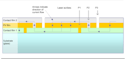
Thin-film solar cells typically consist of three layers deposited on a large glass substrate: a transparent conductive oxide (TCO) layer, a middle semiconductor photovoltaic layer, and a thin metal layer. FIGURE 1 shows a cross-sectional schematic of a typical TFPV device. Semiconductor materials for thin-film solar cells include cadmium sulfide/cadmium telluride (CdS/CdTe), copper indium gallium di-selenide (CIGS), amorphous silicon (a-Si), or a combination of a-Si and microcrystalline-Si (µc-Si) layers.
For CIGS TFPV devices, the metal layer is on the glass substrate, just below the semiconductor film; for CdS/CdTe, a-Si, and µc-Si TFPV devices, the metal layer is above the semiconductor. Typical TCO materials used are indium tin oxide (ITO), tin oxide (SnO2), and zinc oxide (ZnO); typical metal layers are aluminum (Al), gold (Au), copper (Cu), and molybdenum (Mo). Substrates for cell fabrication include several-millimeter thick soda-lime glass as well as polymers and metals with thicknesses in the range of 10s to 100s of microns.
The materials are arranged in a layered structure such that there are two electrically conducting “contact” surfaces (“front-side” facing the sun and “back-side” contacts) with a semiconductor (PV) material as solar absorber in between. Front-side electrical contacts utilize TCO materials, such as ITO or SnO2, which allow both sunlight and electricity to propagate within them with minimal loss.
In the production of a TFPV device, three scribe processes are typically performed (commonly referred to as the P1, P2, and P3 scribes), with various film deposition processes occurring in between. The P1 scribe removes a first electrical contact film from the glass substrate; the P2 scribe removes the solar absorber film from this first contact film; and the P3 scribe removes both the solar absorber layer and a second electrical contact film from the first contact film. The laser scribes divide the large, meter-sized solar panels into several narrow PV cells operating electrically in series. This results in a more practical and efficient low-current, high-voltage device.
The affect of beam quality
Various types of lasers are employed for thin-film scribing, with DPSS Q-switched lasers, at both 1064 nm and 532 nm wavelength, among the most common. Recently, lower cost, more compact pulsed fiber lasers have emerged and been offered as the next-generation solution for laser scribing. While both DPSS and fiber lasers offer short pulses and variable repetition rates, one of the significant differences between the two laser systems is their beam quality or M2 factor. Basically, M2 describes the deviation of the laser beam from a theoretical Gaussian shape; for a theoretical Gaussian beam M2=1; for a real laser beam usually M2>1. A typical DPSS laser system has a superior TEM00 beam profile and beam quality M2 of less than 1.2. Typical first-generation pulsed fiber lasers have an M2 value of greater than 1.8, some even as high as 4.1 Newer generations of pulsed fiber lasers have improved beam quality. However, it remains to be seen if good quality beam, low cost, and compact size can all be achieved within a single system.
In TFPV processing, most scribes are performed with the laser beam incident from the substrate-side of the target film(s). So, any aberrations in the substrate will affect how tightly the laser beam can be focused, thus, the beam intensity at the processing site and ultimately the quality of the scribe. As TFPV panels scale to larger and larger substrates, glass quality and flatness will decrease as manufacturers strive to lower costs. Beam quality will become increasingly important for ensuring robust, high-yield scribe processes that are more forgiving of variations in glass substrate flatness, thickness, and other surface irregularities. In addition, for higher throughput and lower manufacturing cost, lasers will also have to deliver smaller scribe line widths to increase cell efficiency along with higher scribe quality for good electrical isolation.
While it has been shown that shorter pulse widths and higher peak powers help reduce undesired thermal effects such as heat affected zones, material recast, and micro-cracking of the substrate, we have shown that beam quality is also an important factor in choosing a laser system for robust TFPV scribing.
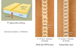
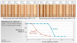
FIGURE 2 shows laser scribes in SnO2 material performed with a Spectra-Physics DPSS HIPPO laser with 17 W of output power, 15-ns pulse durations at 50 kHz, and an M2 of 1.2. Also shown for comparison are scribes achieved using a 20 W, 15-ns pulsed fiber laser with an M2 of 1.8. The laser beam was incident from the glass side and focused at the glass-SnO2 interface. Both lasers seem to adequately cut the P1 scribes with good electrical isolation.Electrical isolation suffered dramatically once the processing occurred far enough away from the beam waist or focal plane location. Because lower M2 values have longer Rayleigh ranges, their processing zones are larger. Therefore, systems with lower M2 beam quality can tolerate higher variations in glass thickness, flatness, and other surface variations, resulting in a more robust laser scribing process.
Summary
Because they can offer significant cost advantages, thin-film solar panels are expected to gain market share in the push for alternative energy. Laser systems will play a critical part in the manufacturability of these thin-film photovoltaics. Lasers are used for scribing the thin-film layers, basically “sculpting” the devices from the conducting and semiconducting layers. Choosing the correct laser system is critical for achieving a high-yield robust process. From the study presented in this article, it is clear that choosing a laser system with a better beam quality, that is lower M2, will deliver better depth of focus to allow precise machining over varying substrate thicknesses for higher yields. Better beam quality will enable a more robust, higher quality scribe process that will increase overall processing efficiency and ultimately lower overall manufacturing costs.
Reference
1. T. Hoult and J. Gabzdyl, “Fiber lasers in the photovoltaic industry”, Industrial Laser Solutions, 24, 11, 2008, pp18-20.


