A team of researchers recently managed to capture the real-time ballistic transport of electrons within graphene at the University of Kansas’ Ultrafast Laser Lab—and it may lead to faster, more powerful and energy-efficient electronic devices in the future (see video).
Electron motion tends to be interrupted by collisions with other particles within solids roughly 10 to 100 billion times per second. This slows the electrons, causes energy loss, and generates excess heat. If these collisions could be prevented, an electron could move unimpeded within a solid akin to a ballistic missile as it travels through air.
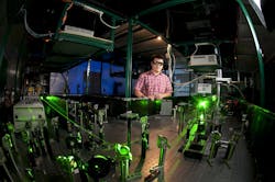
“Ultrafast lasers offer super-high time resolution and are among the fastest experimental tools,” says Hui Zhao, a professor of physics and astronomy (see Fig. 1). “Ballistic transport of electrons in solids occurs on very short time scales, so it’s a perfect match to study ballistic transport via ultrafast lasers to track the motion of electrons.”
Previous electrical measurements had revealed features of ballistic transport, “but it’s cool to actually track their ballistic motion in real time and real space,” Zhao adds. “This provides a noninvasive and nondestructive tool to monitor electrons within solids.”
All-optical ultrafast laser technique
The team observed the ballistic movement in graphene, which consists of a single layer of carbon atoms that form a hexagonal lattice structure. Graphene is hailed as a wonder material because its unusual properties may enable faster and more efficient next-gen electronic devices.
“Light provides energy to an electron to liberate it so it can move freely, leaving a ‘hole’ at its original place,” says Zhao. But electrons in graphene only stay mobile for about one-trillionth of a second before falling back into the hole—which makes it a challenge to track their motion.
To maneuver around this, the team designed and fabricated a four-layer artificial structure with two graphene layers separated by molybdenum disulfide and molybdenum diselenide. “By inserting two monolayer semiconductors between two graphene layers, we separate electrons and holes so the electrons don’t fall back into the holes as quickly, which gives us a sufficient time window to analyze the nature of the electron motion,” says Zhao.
The two layers of molecules with a total thickness of just 1.5 nm “forces the electrons to stay mobile for about 50-trillionths of a second,” says Ryan Scott, a Ph.D. student, who ran the experiments. This is enough time for researchers, equipped with lasers as fast as 0.1 trillionth of a second, to track the electrons’ movement.
The team’s measurement setup, a transient absorption microscope based on ultrafast lasers, can resolve the motion of electrons with nanometer-scale spatial resolution. “Our technique tracks mobile electrons in graphene by their effect on light reflection—they slightly increase the reflectance of the sample at their locations,” says Zhao. “This allows us to use a laser pulse to track them as they move.”
In other words: they use a tightly focused laser pulse called a “pump pulse” to liberate electrons within their sample, which they trace by mapping out the reflectance of the sample with another focused laser pulse called a “probe pulse” that arrives at the sample at a slightly later time.
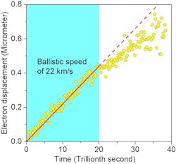
To detect such a small change, they liberated 20,000 electrons at once and used the probe laser to reflect off the sample and measure this reflectance. The team repeated the process 80 million times for each data point. Figure 2 shows an example of their key results in a displacement vs. time graph of a tiny electron, and the straight line means motion with constant velocity. So the researchers conclude the electrons, on average, move ballistically for about 20-trillionths of a second, with a speed of 22 kilometers per second, before running into something that terminates their ballistic motion.
Compared to electrical detection techniques, their all-optical ultrafast laser technique offers the high resolution necessary to explore electron transport within ballistic and coherent regimes.
One of the most surprising aspects of the team’s work was when their initial tests confirmed the design of their device structure works. “The electrons are indeed separated from the holes by the two monolayers and stay mobile for a longer time,” says Zhao. “So we knew we had a good chance to track their ballistic motion. Our group has been studying charge transfer in types of van der Waals heterostructures for 10 years, so it’s exciting to see that we can use these artificial structures to fine control the electrons and make them stay mobile longer.”
Biggest challenge? Since the optical signal is weak, the team had to average many measurements to get conclusive features. “This requires the experimental setup to be stable for a long period of time,” says Zhao. “It took some tricks and tedious work to get it done.”
Going ballistic
The really great news: ballistic electron transport is fast and free of scattering (energy loss), so electronic devices using ballistic transport can potentially be much faster, as well as more powerful and energy-efficient—reducing latency and heat issues.
“Now that we have a ‘radar gun’ to monitor ballistic electron motion, we’ll try to use it as a tool to study how to control the electron motion with electric fields and other means,” says Zhao. “We’d also like to explore new device designs to prolong the ballistic transport length of electrons. The samples in this study were kept at room temperature. Cooling the sample down to lower temperatures could also prolong their ballistic length.”
This project is supported by the U.S. Department of Energy, and Ryan Scott’s work is supported by the Redeker fellowship and graduate research award of University of Kansas.
FURTHER READING
R. J. Scott, P. Valencia-Acuna, and H. Zhao, ACS Nano, 17, 24, 25368–25376 (2023); https://doi.org/10.1021/acsnano.3c08816.


