NORMAN HODGSON, MICHAEL LAHA, TONY S. LEE, ALBRECHT STEINKOPFF, and SEBASTIAN HEMING
Over the last five years, material processing with femtosecond pulses in the range of 300 to 900 fs has gained in popularity due to the small heat-affected zone (HAZ) and increased energy penetration depth resulting from the high laser pulse intensity. Industrial ultrashort-pulse (USP) diode-pumped solid-state and fiber lasers are now being used to cut foils for flat panel displays, to cut stents, and to drill fuel injector nozzles, as well as for wafer scribing and surface microstructuring.
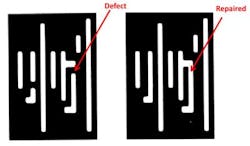
The first industrial use of femtosecond laser pulses for microprocessing dates back to the late 1990s, where titanium sapphire (Ti:sapphire) amplifiers were used to repair lithography masks in integrated circuit fabrication. At that time, the only choice in commercial laser sources were Q-switched, neodymium (Nd)-doped solid-state lasers delivering pulse duration of tens of nanoseconds, and ultrafast Ti:sapphire amplifiers that exhibited pulse durations of 100 fs and provided output power at the 1 W level at 1 kHz (FIGURE 1). The small feature size of the chromium layer on top of the fused silica substrate prohibited the use of nanosecond pulses due to thermal damage of the chromium, and even the substrate. The necessity for a small HAZ outweighed the high cost of a Ti:sapphire amplifier system, which was about $300,000.
FIGURE 1. Lithography mask repair using a 100 fs Ti:sapphire laser is shown, where a chromium layer on a fused silica substrate is ablated; width of the ablated lines is 750 nm.1
Today, many different femtosecond lasers are available, providing output pulse energies of up to 200 µJ, with average output powers in the kilowatt range. Especially over the last decade, a large variety of femtosecond solid-state laser and fiber laser architectures have entered the material processing field, all of them based on ytterbium (Yb)-doped gain materials. Average output powers of up to 100 W are currently employed in industrial applications, with pulse durations between 300 and 900 fs and repetition rates of up to 2 MHz. Compared to the original Ti:sapphire amplifier systems, the output powers have increased by two orders of magnitude, while system cost has been considerably decreased at the same time.
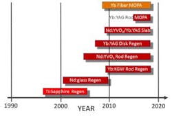
A majority of the low-power lasers have been deployed in ophthalmic applications. In the 2000s, Nd:glass regenerative amplifiers were used to cut the corneal flap in LASIK surgery by generating a bubble plane inside the cornea. These Nd:glass systems were later replaced by Yb:fiber master-oscillator power-amplifiers (MOPAs), which allowed higher repetition rates at a lower cost (FIGURE 2). Typical pulse energies required for flap cutting are 2–4 µJ at repetition rates of 50 to 200 kHz and pulse durations of around 300 fs. A second, more recently emerging ophthalmic application is lens dissection as part of cataract surgery. In this case, the pulse energies employer are in the range of 20 to 40 µJ at repetition rates of 50 to 100 kHz, and pulse durations are preferably below 800 fs.
FIGURE 2.The evolution of the deployment of femtosecond lasers in microprocessing applications is shown; Ti:sapphire regenerative amplifiers for mask repair have been replaced by picosecond Nd:YVO4 lasers and Nd:glass regenerative amplifiers by femtosecond Yb fiber MOPAs.
According to a forecast by Strategies Unlimited in 2016, the total market in 2019 for femtosecond and picosecond lasers used for material processing (including ophthalmic applications) is projected to be $460 million (TABLE 1).2 Half of this revenue is generated by picosecond lasers, which have been widely used in microelectronic manufacturing. The other half is split between ophthalmic femtosecond lasers ($136 million) and femtosecond lasers for non-biological material processing ($98 million).
TABLE 1. The 2016 Revenue Forecast of femtosecond and picosecond lasers in material processing is shown, where values for 2014 and 2015 are actual revenues; femtosecond lasers include ophthalmic lasers.2
Mechanism and benefits of femtosecond laser processing
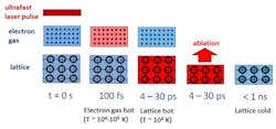
The interaction of femtosecond and picosecond pulses with matter is governed by the absorption of the light by the electrons and subsequent energy transfer to the lattice. In the case of metals, the photons are absorbed by the electron gas, which increases its temperatures to values of several 10,000°C. The electrons will transfer their energy to the lattice within the electron-phonon relaxation time, which for most materials is in the range of 100 fs to 1 ps at room temperature. The lattice has about 100X higher heat capacity compared to the electrons. This leads to a substantial delay between the incidence of the laser pulse and the time when the lattice has reached melting temperature (FIGURE 3). For high laser fluences, the ablation of the heated material occurs several tens of picoseconds after the laser pulse is absorbed.
FIGURE 3.Interaction of ultrafast pulses with a metal is shown. The electron gas absorbs the laser light, leading to a hot, thermalized electron distribution within 100 fs; the lattice will heat up with a delay of 4 to 30 ps.
The light-matter interaction for ultrashort laser pulses can be mathematically described by the Two-Temperature Model, which provides the temporal and spatial evolution of the temperature of electron gas and lattice by incorporating the coupling between both systems via the electron–phonon relaxation time.3 This model has been used very successfully over the last decades to calculate damage threshold fluence, ablation rates, and HAZ for ultrashort pulse processing (FIGURE 4).4-8 The main results are that for pulses that are shorter than 10 ps, the damage threshold fluence remains constant, while for larger pulse durations, the threshold fluence increases in proportion to the square-root of the pulse duration, independent of incident laser pulse wavelength.
FIGURE 4.Calculated temporal temperature distribution of electron gas (left) and lattice for copper after irradiation with a 100 fs pulse at an average fluence of 0.14 J/cm2 and a wavelength of 800 nm.7
Similarly, the HAZ remains constant for pulse durations below 10 ps, again independent of the wavelength of the laser light. The basic reason for this behavior is the delay in the temperature increase of the lattice and of heat conduction into the material. This regime of pulsed laser-matter interaction is therefore referred to as cold ablation, since the lattice stays cold during irradiation by the laser pulse. This name is a bit misleading, though, since the material will have to reach melting temperature to induce ablation.
The most interesting effect of ultrashort pulse interaction, however, is the increase in the energy penetration depth and ablation depth with decreasing pulse duration. Decreasing the pulse duration at a given energy fluence leads to an increase in the temperature of the electron gas and a simultaneous increase of the electron-phonon relaxation time.
In a more mechanical model, this can be easily understood: the velocity of the electrons traveling through the lattice can become as high as 100,000 m/s for femtosecond pulses due to the very high intensity, and this high speed results in deeper penetration of the electron into the lattice without transferring energy to the lattice.8
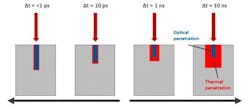
The material processing efficiency and quality depends on the duration of the laser pulses. For pulses in the nanosecond regime, the absorption of the laser pulse is determined by the linear optical absorption depth of the laser light and the energy dissipation is a result of heat conduction into the material (FIGURE 5). For pulses that are shorter than 10 ps, the initial energy penetration depends strongly on the light intensity and leads to deeper penetration depth for femtosecond pulses. In addition, the lack of thermal conduction during the pulse and the time of lattice heating results in a very low HAZ. For metals, HAZ of less than 5 µm can be achieved, while for plastic materials, the HAZ is typically in the range of 30 to 50 µm.
FIGURE 5. Absorption of a laser pulse in a medium is shown, where energy penetration is represented in blue and volume heated via heat conduction in red.
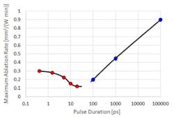
The increase of the penetration depth for shorter pulses leads to an increase in the maximum ablation rates when the pulses become shorter than about 20 ps (as shown in FIGURE 6 for aluminum). As will be discussed subsequently, at any pulse duration the maximum ablation rate is achieved at a pulse fluence of about 7.5X the ablation threshold fluence. Compared to Q-switched laser pulses with pulse durations of tens of nanoseconds, the increased electron velocity in the material leads to ablation rates for sub-picosecond pulses that are only a factor of three lower.
FIGURE 6. Maximum ablation rates of aluminum with Coherent's measured values (red dots) and using values taken from data published by Breitling et al. (blue dots).9
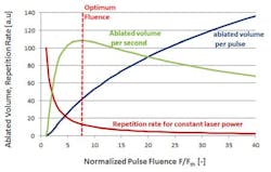
For pulsed lasers, ablation becomes most efficient at a pulse energy fluence equal to e2 times the threshold fluence. This is a result of the saturation of the ablated volume with increasing pulse fluence. At a fixed output power, more volume can therefore be ablated if the energy fluence is lowered, while simultaneously increasing pulse repetition rate and therefore throughput (FIGURE 7). The maximum value is achieved at the optimum fluence. The ablation rate, C (in mm3/W/min), is given by:
where F is the peak fluence in J/mm2, Fth is the peak threshold fluence, and d is the energy penetration depth per pulse in millimeters.10 Typical values for the energy penetration depth per pulse are in the range of 20 to 100 nm for metals, semiconductors, and plastics, and >500 nm for glasses and transparent crystals.
FIGURE 7. Ablated volume per pulse (blue curve) and ablated volume per second (green curve) at constant laser power are shown.10
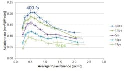
FIGURE 8 shows the measured ablation rates for Nitinol as a function of the average pulse fluence for various pulse durations. Nitinol is used to manufacture stents and requires femtosecond pulses to increase the throughput. The laser was a 1035 nm modelocked fiber MOPA, where the settings of the compressor were changed to implement different pulse durations, and external second- and third-harmonic generation (SHG and THG, respectively) stages could be added to access wavelengths of 517 and 345 nm. A rectangular area of about 0.5 × 1.5 mm was ablated to a depth of about 200 µm using a spot diameter of 20 µm with a spot overlap of 60% in both directions. Decreasing the pulse duration to 400 fs resulted in an increase in the ablation rate by a factor of two compared to 19 ps pulses. This increase in ablation efficiency for femtosecond pulses is common amongst metals and semiconductors. For transparent dielectrics, however, the ablation rate is higher for picosecond pulses. This is due to the lack of free electrons, which requires high threshold fluences to ablate the material. For femtosecond pulses, the resulting peak powers are too high and lead to optical breakdown and decreased ablation rates.
FIGURE 8. Measured ablation rates of Nitinol at 1035 nm as a function of average pulse fluence are shown; the parameter is the pulse duration.
Ablation rates vary with laser wavelength, depending on the absorption spectrum of the material. In general, the ablation rates become higher when the material already has a linear absorption at the incident wavelength.
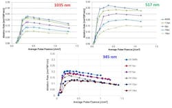
FIGURE 9 shows steel ablation rates for infrared (IR), green, and ultraviolet (UV). While the ablation rates for the 517 nm laser are 50% higher as compared to IR, there is also a 2X decrease in laser efficiency when converting an IR laser to green emission using extra-cavity SHG. Considering typical conversion efficiencies of 50% and 30% for green and UV generation, respectively, there are not many materials where using harmonic wavelengths will increase the absolute value of the ablation rate. Exceptions are aluminum, Nitinol, and gold for green emission wavelengths, and plastic materials (PET, OLED layers, polarizers, etc.), where UV will lead to increased ablation and better cut quality. In all other cases, the biggest benefit of using harmonic wavelengths is the increased Rayleigh range, which results in an increased depth of field or in smaller kerf widths.
FIGURE 9.Measured ablation rates for steel at different wavelengths as a function of energy fluence and pulse duration are shown.
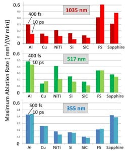
The comparison of maximum ablation rates for a variety of materials for 10 ps and 400 fs pulses at three different laser wavelengths is presented in FIGURE 10. While there are variations in ablation rates between different wavelengths, the variations are relatively small, and the choice of wavelength is more determined by focusing conditions and the linear absorption of the material. Exceptions are transparent materials that require IR laser wavelengths at pulse durations of tens of picoseconds.
FIGURE 10.Measured maximum ablation rates for various materials at IR, green, and UV laser wavelengths and two different pulse durations of 10 ps/400 fs for IR and green, and 10 ps/500 fs for UV are shown.
Note that the typical ablation rates are on the order of 0.2 mm3/(W min), which means that with a 100 W laser, the equivalent volume of a 10-cent U.S. coin piece can be ablated within about 2 minutes of laser-on time.
Increased throughput with burst mode
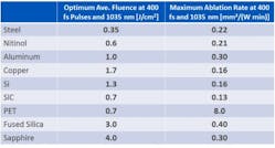
One of the challenges of USP laser material processing is that maximum ablation rates are achieved at relatively low average pulse fluences. TABLE 2 provides an overview of the measured optimum (maximum ablation rate) average pulse fluences for various materials. With the exception of transparent dielectrics, the optimum fluences are on the order of 1 J/cm2 or lower.
TABLE 2.Measured optimum average pulse fluences and maximum ablation rates for 400 fs pulse duration and a wavelength of 1035 nm are shown.
However, achieving these low optimum fluences (and therefore optimum ablation rates) in practice is problematic. For example, a laser with an output power of 50 W at a 500 kHz repetition rate will yield an average energy fluence of 14 J/cm2 at the work surface when focused to a 30 µm spot diameter. Operating at this high fluence results in a much lower ablation rate, as well as an increased HAZ, since the heat-affected area increases with increasing pulse fluence. To approach the optimum fluence, the laser has to be either focused to a 3–5X larger spot size, which in many cases would be too large, or alternately, be operated at 10-20X the repetition rate, which is prohibited by the current scanner technology.
A solution to this problem is provided by operating in so-called seeder burst mode. To understand seeder burst mode, realize that all industrial USP lasers are based on a modelocked seed laser, which typically operates at a repetition rate of about 50 MHz. To produce 500 kHz final output (as in the preceding example), a pulse picker separates out every hundredth pulse and amplifies it. The rest of the pulses are discarded.
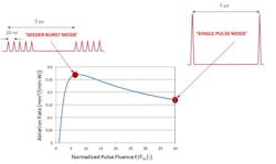
In one implementation of seeder burst mode, instead of picking out every hundredth pulse, a train of 3 to 10 pulses, each of which are about 20 ns apart, is utilized. As a result, the individual pulse fluence is reduced by a factor of N, where N is the number of pulses in the burst, while the average power of the laser remains constant (FIGURE 11). This allows operation at, or near, the optimum fluence to produce a substantial increase in ablation rate. Also, note that the pulse separation is sufficient so that, for metals and semiconductors, the lattice returns to its initial temperature between pulses, meaning individual pulses hit the cold target again. This is also true for most glasses, where the workpiece is ‘cold’ after <10 ns.
FIGURE 11.Change in ablation rate at constant laser power by using a burst of 5 seed pulses instead of a single pulse at 200 kHz is shown.
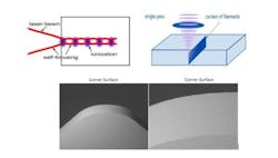
Burst mode has a different effect when cutting deep trenches, as the plasma generated cannot escape and will interact with the subsequent pulse. In this case, there is interaction between the individual laser pulses via absorption in the plasma.11,12 This effect is used with picosecond and femtosecond lasers for filament cutting of glasses, where long filaments with diameters of several microns are generated through a balance of self-focusing and de-focusing after plasma generation (FIGURE 12). Since the plasma lifetime is on the order of 30 ns, a seeder burst mode with seed frequency of 50 MHz or greater will generate an interaction of the next laser pulse with the plasma generated by the previous one, leading to a long chain of focusing and defocusing events inside the material. By placing filaments next to each other, glasses can be cut at speeds of meters per second with thicknesses of up to 5 mm, and surface roughness of <0.3 µm RMS. Filament cutting is used in the automotive and aviation industries to cut window glass and mirror glass.
FIGURE 12.Filament cutting of glass by generating long filaments inside the material via self-focusing and de-focusing by the generated plasma is shown; close positioning of the filaments leads to smooth cut surfaces with a roughness of <0.3 µm RMS.
Building reliable USP lasers with burst mode
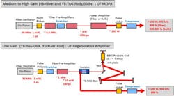
While all industrial femtosecond laser amplifiers are based on Yb-doped crystals or fibers, there are two distinct amplifier architectures used depending on the geometry of the gain materials they employ (FIGURE 13). For amplifiers based on fibers, slabs or multi-rod systems, the gain per pass is high enough to use a MOPA architecture, where a seed laser providing power of tens of milliwatts (for fibers), and several watts for slabs and rods, at repetition rates of around 50 MHz is pulse-picked and then amplified to more than 100 W. The MOPA architecture has several advantages, like operation at high repetition rates up to tens of megahertz, easy implementation of seeder burst mode, and power-scaling by adding additional amplifier stages.
FIGURE 13. The two laser architectures used for industrial femtosecond lasers are MOPA for fibers, slabs, and multi-rod systems (top) and regenerative amplifier for low-gain systems (disks and single rods; bottom); both architectures use CPA.
For amplifiers utilizing Yb:YAG disk lasers and single rods, the gain per pass is too low to get enough amplification of the seed laser, and regenerative amplifiers are used to achieve the 100+ W output power. For Yb:YAG disks, the seed pulses are switched into the amplifier cavity via a Pockels-cell, and the pulse makes about 150 round-trips inside the resonator before the Pockels-cell ejects the high energy pulse again. Regenerative amplifiers are limited in repetition rate to ~1 MHz (due to the Pockels-cell switching electronics) and it is difficult to implement seeder burst mode in this architecture. For this reason, MOPA architectures have a clear advantage for femtosecond and picosecond material processing (TABLE 3).
TABLE 3. Operating parameters of employed industrial femtosecond lasers are shown; all three systems have a demonstrated power-scaling capability of kilowatts, but only up to 100 W output power is currently being used.
Independent of the amplifier architecture (MOPA or regen), all USP laser systems use chirped pulse amplification (CPA) to stretch and compress the pulse after amplification. A femtosecond laser therefore will also provide picosecond pulses by changing the compressor settings—a distinct advantage when optimizing a given process by varying the pulse duration.
Since 2015, Coherent has offered a family of femtosecond fiber-MOPA-based laser products under the name MONACO. Average powers of up to 60 W, pulse energy of up to 80 µJ, and tunable pulse durations between 300 fs and 10 ps, plus easy access to burst mode operation, make the MONACO lasers the ultimate tool for ultrashort laser processing. Models with green and UV output wavelengths are also available.
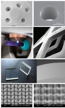
FIGURE 14. Industrial applications of femtosecond lasers include injector nozzle cutting, stent cutting, glass filament cutting, and microtexturing of metals.
Applications
At present, femtosecond lasers are used in a variety of applications that require the creation of small structures with low HAZ and high quality of the ablated surface areas. While the majority of new femtosecond laser installations are still for ophthalmic applications, the non-biologic material processing market has seen double-digit growth over the last couple of years. Some of the main applications are shown in FIGURE 14. There is particularly strong growth in the semiconductor and display markets, where femtosecond and picosecond lasers are used to cut foils used in flat panel displays (FIGURE 15) and for thin wafer scribing.
FIGURE 15.UV picosecond and femtosecond lasers are used to cut OLED foil; the UV wavelength generates lower HAZ and cleaner cuts in plastic foils as compared to IR laser pulses.
It is estimated that the non-biological microprocessing portion of femtosecond and picosecond laser market will grow at a CAGR of 13%, leading to a total revenue of $675 million in 2025.2 In addition, about $200 million of ophthalmic femtosecond lasers are expected to be sold annually by 2025, representing a 6% CAGR.
Over this time period, higher-power femtosecond lasers providing several hundreds of watts will enter the industrial application space, and new USP processing techniques will emerge, especially for cutting multilayered structures, processing novel compound materials, and laser cutting of smartphone display glass. At present, all smartphone display glasses are cut mechanically using diamond wheels and grinders. Once an all-laser solution for display glass cutting is found (this includes not only cutting the periphery, but also chamfering and cutting the holes for speakers and homing button),13 the growth of industrial femtosecond lasers may far exceed the 13% projected CAGR.
REFERENCES
1. N. Hodgson et al., "Diode-pumped TEM00 mode solid state lasers and their micromachining applications," Proc. SPIE, 4977, 281 (2003).
2. Strategies Unlimited, The Worldwide Market for Lasers: Market Review and Forecast 2016; https://store.strategies-u.com/the-worldwide-market-for-lasers-market-review-and-forecast-2016.
3. S. I. Anisimov et al., Sov. Phys. JETP, 39, 375 (1974).
4. N. K. Sherman et al., Opt. Eng., 28, 10, 1114 (1989).
5. T. Q. Qiu et al., Int. J. Heat Mass Transfer, 35, 3, 719 (1992).
6. S. Nolte et al., J. Opt. Soc. Am. B, 14, 10, 2716 (1997).
7. J. Byskov-Nielsen, "Short-pulse laser ablation of metals: Fundamentals and applications for micro-mechanical interlocking," PhD thesis, Univeristy of Aarhus (2010).
8. S.-S. Wellershoff et al., Appl. Phys. A, 69, 99 (1999).
9. D. Breitling et al., "Fundamental aspects in machining of metals with short and ultrashort laser pulses," Proc. SPIE, 5339 (2004).
10. B. Neuenschwander et al., "Optimization of the volume ablation rate for metals at different laser pulse-durations from ps to fs," Proc. SPIE, 8243 (2012).
11. S. Rezaei, "Burst-train generation for femtosecond laser filamentation-driven micromachining," PhD thesis, University of Toronto (2011).
12. D. Esser et al., Opt. Express, 19, 25, 25632 (2011).
13. T. S. Lee, "High speed glass cutting at oblique angles," ICALEO 2018, Talk M701 (Oct. 17, 2018).
NORMAN HODGSON([email protected]) is vice president of technology and advanced research,MICHAEL LAHA ([email protected]) is product line manager for ultrafast industrial lasers, and TONY S. LEE([email protected]) is senior applications engineer, all at Coherent, Santa Clara, CA, www.coherent.com, while ALBRECHT STEINKOPFF, engineering intern, is now with the Institute of Applied Physics at the University of Jena, Jena, Germany, andSEBASTIAN HEMING, engineering intern, is nowwith the University of Münster, Münster, Germany.

