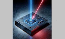
Today’s electronic devices tend to operate within the gigahertz range, but next-gen electronics are already pushing into millimeter waves, so prototypes of high-speed transistors, hybrid photonic platforms, and terahertz metadevices need to be able to bridge the electronic and optical domains.
Characterizing and diagnosing these next-gen devices is a challenge if you don’t have the diagnostic tools you need available—particularly in terms of speed and spatial resolution. So a team of University of Konstanz researchers set out to create a tool to capture space-time imaging of electronic circuitry at the femtosecond/terahertz domain (see Fig. 1 and video).
“Information is ubiquitous in our modern world, and electronic devices are the main means to process it,” says Peter Baum, a physics professor whose Light and Matter team created the imaging method. “Circuitry must therefore become smaller and faster all the time. But if you make a record-fast device, how do you actually measure it? This is a chicken-egg type of problem that needs to be solved.”
Femtosecond electron beam probe
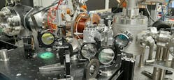
To create a tool to help solve the chicken vs. the egg challenge, Baum’s team developed a method that uses an ultrafast electron microscope to measure electric potentials as a movie in space and time.
Essentially, they create femtosecond electron pulses in a transmission electron microscope, compress them with infrared laser light to 80-fs duration, and synchronize them to the inner fields of a laser-triggered electronic transmission via a photoconductive switch.
Their pump-probe method allows the researchers to directly sense the local electromagnetic fields of their electronic devices as a function of space and time.
The team’s ultrafast electron beam probe provides femtosecond, nanometer, and millivolt resolutions—and doesn’t affect in situ operation of the device (see Fig. 2).
“A femtosecond laser creates femtosecond electron pulses that are much shorter than almost any electronic process that can happen within a device,” says Baum. “Like in a stroboscope, the dynamics under investigation become apparently frozen and can then be visualized. Importantly, the electronic device’s operation isn’t distorted by the diagnostics in any way, so we can measure it under normal operation conditions.”
One remaining challenge involved in this work is specimen preparation. “The substrate needs to be thin enough so that the electron beam can pass through it,” says Baum. “Circuitry usually consists of multiple layers and thinning it out isn’t always straightforward. But the top layers are the smallest and fastest—and they’re thin enough.”
The team’s femtosecond electron beam probe method is poised to open new avenues of R&D into next-gen electronics because diagnostic resolutions are now limited only by the de Broglie wavelength of electrons in the microscope and the cycle time of the far-infrared laser light applied for all-optical electron pulse compression.
“Computer chip production is already relying heavily on electron microscopes for quality control,” says Baum. “Our new method for space-time imaging of electronic circuitry at the femtosecond/terahertz domain can be easily integrated into these apparatuses and our methods can become widespread.”
Baum hopes for a better understanding of fundamental functionality and mechanisms behind the workings of ultrafast circuitry. “Our movie-like measurements can guide the design and fabrication of innovative devices as efficiently as possible toward breakthrough innovations and discoveries.”
Meanwhile, Baum’s team is also working to extend their methods to the genuine optical regime. “We need attosecond time resolution to see the optical cycles of light oscillate and propagate,” he says. “When electronics eventually become so fast that they merge with optical technologies, we’ll be ready to see it in space and time.”
FURTHER READING
M. Mattes, M. Volkov, and P. Baum, Nat. Commun., 15, 1743 (2024); https://doi.org/10.1038/s41467-024-45744-8.
D. Nabben et al., Nature, 619, 63–67 (2023); https://doi.org/10.1038/s41586-023-06074-9.


