by Lonnie Lucas and Jim Zhang, Applied Energetics
A review of laser sources, basic mechanisms, and potential applications
The title above immediately leads to two questions: What is a femtosecond laser, and what is laser micromachining? Let’s start by discussing the first question.
Femtosecond lasers
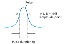
Femtosecond (fs) lasers are also commonly known as ultrafast and/or ultrashort-pulse (USP) lasers. Two important parameters used to describe femtosecond lasers are pulse duration (width) and pulse repetition rate (PRR). The pulse duration (tp), shown in FIGURE 1, is also referred to as full width at half maximum (FWHM) amplitude.
The pulse repetition rate (PRR) describes the frequency with which pulses are emitted by the laser. For instance, in FIGURE 2, if the PRR was 1 kHz, then the period T would be equal to 0.001 seconds (T= 1/PRR).
Thus, when we are discussing a femtosecond laser, it has a pulse duration (tp) in the 1-999 fs regime. Some of the more common time scales used with lasers are shown in the table below.
A femtosecond (10-15 seconds) is one quadrillionth, or one millionth of one billionth of a second. Put another way: a femtosecond compares to a second, as a second compares to 30 million years.
A couple of other parameters are useful when discussing ultrafast lasers: peak power (Ppeak) and average power (Pavg). Peak power = pulse energy / pulse duration. Average power = pulse energy * pulse repetition rate.
For the case of Ep =5 mJ in tp= 100 fs, the peak power of such a laser would be 50 gigawatts (GW), many times more than what a large electrical power plant delivers (about 1 GW). When focused by a lens, these laser pulses will destroy any material placed in their focus, even air molecules.
Laser micromachining
The market originally viewed the femtosecond laser much as “conventional wisdom” perceived the Internet back in the early 1990s: hardly anybody anticipated that so many people around the world would depend on it, and for such a range of uses. But after 20 years of femtosecond R&D, this laser is now finding applications in “cold” ablation, notably the drilling and cutting of high-precision holes (such as in the production of medical stents) free from thermal damage. The ultrafast lasers essentially vaporize matter without generating heat, creating new ways to machine materials. They are particularly good at machining very small, very precise patterns in tough materials.1
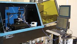
FIGURE 3 shows the Applied Energetics Laser Microfab (µFAB), a tabletop laser microfabrication workstation designed for use in laser ablation, surface structuring of tough materials, writing of waveguides, and microfluidics. Relevant industrial materials often used in ablation applications include metals, polymers, semiconductors, glasses, and ceramics.
Types of ultrafast lasers
Ultrafast laser micromachining is a process by which pulses from an ultrafast (pulse duration less than a few picoseconds) laser are used to induce micrometer-sized structures on the surface or in the bulk of solid materials.2-6
Pulsed solid-state lasers
The most common lasers used today for micromachining are solid-state ultrafast lasers, with gain media such as:
- Titanium-doped sapphire (Ti:Sapphire)
- Ytterbium-doped yttrium aluminum garnet (Yb:YAG)
- Ytterbium-doped potassium gadolinium tungstate (Yb:KGW)
- Ytterbium-doped potassium yttrium tungstate (Yb:KYW)
The Ti:Sapphire laser uses a titanium-doped sapphire crystal as the gain medium, has a center wavelength near 800 nm, and is capable of very short (<10 fs) pulse generation. The Yb-doped YAG or tungstate lasers use a ytterbium-doped yttrium aluminum garnet (YAG) or a ytterbium-doped potassium yttrium tungstate (KYW) or potassium gadolinium tungstate (KGW) crystal as the gain medium and have a center wavelength of near 1.0 µm.
The Yb:YAG or Yb:tungstate lasers can be pumped by a diode laser, and therefore the Yb-doped laser systems can be made more compact and at relatively lower cost. FIGURE 4 shows one example of a commercial Yb:KYW ultrafast laser made by Applied Energetics Inc.7
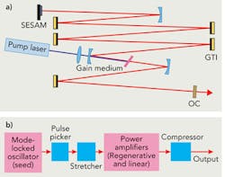
In general, there are two types of ultrafast solid state lasers used for laser micromachining: a mode-locked oscillator only, and a mode-locked oscillator seed followed by chirped pulse amplification (CPA) including a regenerative or linear amplifier. Typically, the mode-locked oscillator alone has a 10 MHz pulse repetition rate and 10 nJ output pulse energy. The CPA laser is capable of pulse repetition rates ranging from a few kHz up to 100 kHz and pulse energies of a few mJ. The schematic configurations for both ultrafast solid-state lasers are shown in FIGURE 5.
Fiber lasers
Fiber laser technology has made dramatic progress in the past decade regarding output power and ultrashort-pulse achievements. Kilowatt output power and greater have been demonstrated for continuous wave (CW) single mode fiber lasers. Pulse energies of >10 µJ are now available for commercial ultrafast fiber lasers.8-9
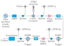
Common fiber laser products on the market are Yb-doped fiber lasers, which use ytterbium-doped silica single-mode fibers (or a large effective area fiber) as the gain medium with a center wavelength near 1030 nm. The core diameter for standard single-mode fibers is a few micrometers and the core diameter for large effective area fibers is about 30 µm. A high (>1 W) average power ultrafast fiber laser is typically composed of a fiber oscillator (a mode-locked fiber seed), a pulse stretcher, a pulse picker, a couple of stages of fiber amplifiers, and a pulse compressor.
The fiber oscillator has typical pulse energy output of ~100 pJ and ~10 MHz pulse repetition rate. For an amplified ultrafast fiber laser, its typical output has a pulse duration of several hundred femtoseconds, a pulse energy of ~10 µJ, and a pulse repetition rate of 10-100 kHz. A schematic of a typical ultrafast fiber laser is shown in FIGURE 6.
The advantages of fiber lasers are their compact size, good beam quality, and high mechanical stability. The disadvantages of fiber lasers, especially ultrafast lasers, are their peak power limitations and nonlinear effect influence. As is well known, ultrafast lasers have very high peak power and the fiber gain media have very small physical diameter and long physical length. So, even with moderate pulse energy, the pulse fluence inside the fiber is very high and nonlinear effects (such as self-phase modulation, Raman scattering, etc.) usually appear. The result is that the pulse temporal profile from the ultrafast fiber laser has a large “pedestal background” — that is, a big portion of the pulse energy is distributed within a much longer time duration.
Micromachining
Setup of equipment
To achieve desired high-quality laser microprocessing results for specific materials, one must select a suitable ultrafast laser and set correct laser operating parameters such as:
- laser wavelength
- repetition rate
- average power
- pulse fluence
- pulse duration
- beam focus
- spot size and quality
- sample moving speed
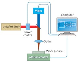
Since materials such as metals, polymers, semiconductors, and transparent materials have dramatic differences in their optical and thermal properties, it is expected that the ultrafast laser operating parameters used for achieving desired processing results must be set differently for each type of material. FIGURE 7 shows a typical schematic setup for ultrafast laser micromachining.
Basic mechanisms of ultrafast laser material processing
Ultrafast laser micromachining is dramatically different from conventional laser processing which uses either a continuous wave (CW) laser or longer microsecond (10-6) pulsed lasers. The big difference comes from the basic principle or mechanisms of laser-induced material removal processes.
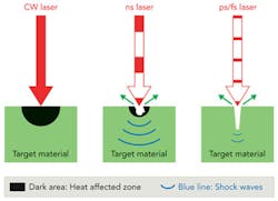
For long-pulsed lasers, ablation of materials occurs through melt expulsion driven by the vapor pressure and the recoil pressure of light. This is an unstable process in which the dynamics of the fluid phase and the driving vapor conditions are quite complicated. The melt layer is resolidified, resulting in geometric changes to the holes (i.e. rough holes).
FIGURE 8, from left to right, shows continuous wave (CW), nanosecond (ns), and pico/femtosecond (ps/fs) laser pulses. The black area indicates the size of the heat-affected zone (HAZ). The blue lines show the shock waves created by the light pulses. The CW laser (far left) removes material primarily by melting, which creates a large HAZ. The (ns) laser pulses (center) create a smaller HAZ and material is removed by melt expulsion driven by the vapor pressure and the recoil pressure. With ultrafast pulses (ps/fs), the laser pulse duration is much shorter than the timescale for energy transfer between free electrons and the material lattice. So, extremely high pressures and temperatures can be attained in a very small (µm) depth. However, the absorbed energy heats the material very quickly past the melting point, directly to the vapor phase with its high kinetic energy. The material is removed by direct vaporization away from the surface without formation of a recast layer. This provides negligible HAZ and very fine, sharp features.
For ultrafast lasers, energy deposition occurs on a timescale that is short compared to atomic relaxation processes. The laser energy is absorbed by the electrons, leaving the ions cold, and only after the laser pulse is gone does thermalization take place. Also, the intensity of a femtosecond pulse is high enough to drive highly nonlinear absorption processes in materials that do not normally absorb at the laser wavelength.
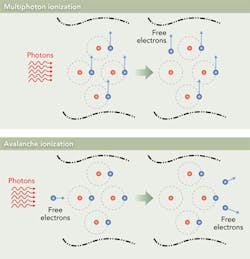
At the high intensities (typically > 1013 W/cm2) of femtosecond lasers, multiphoton ionization becomes significantly strong. As shown in FIGURE 9 (top) for multiphoton ionization, several photons “simultaneously” strike a bound electron due to the very high photon flux of femtosecond lasers. A bound electron is freed from the valence band by absorbing several photons when the total energy of the absorbed photons is greater than the ionization potential. Hence, if laser intensity (photon flux) is very high, multiphoton ionization can be significant. At intensities above 1013 W/cm2, multiphoton ionization becomes considerably strong and seed electrons are not required to initialize ionization in wide-bandgap materials. Wide-bandgap materials are those having a large energy difference (e.g, >5 eV) between the top of the valence band and the bottom of the conduction band. (See Glossary below.)
As shown in FIGURE 9 (bottom), if the kinetic energy of a free electron becomes sufficiently high by absorbing photons, part of the energy may transfer to a bound electron by collisions to overcome the ionization potential and produce two free electrons — this is called (collisional) impact ionization. Consequently, the free electrons absorb photons and produce more free electrons from the bound electrons. Such a series of impacts is called avalanche ionization, where free electron density exponentially increases. Avalanche ionization strongly depends on free electron density, and is sometimes assumed as linearly proportional to laser intensity. Its efficiency is determined by competition between energy gain through inverse Bremsstrahlung and energy loss through phonon emission. Avalanche ionization is responsible for the ablation of wide-bandgap materials at laser intensities below 1012 W/cm2.
The dissipation of the absorbed energy in bulk material, and the corresponding material removal, takes place mostly after the laser pulse duration. Two major mechanisms have been studied: 1) thermal vaporization, where the electron-phonon collisions increase the local temperature above the vaporization point, and 2) Coulomb explosion, where excited electrons escape from the bulk materials and form a strong electric field that pulls out the ions within the impact area.
According to these two mechanisms of material removal, femtosecond laser ablation can be divided into two regimes: strong ablation dominated by thermal vaporization at intensities significantly higher than the ablation threshold, and gentle ablation governed by the Coulomb explosion near the ablation threshold.
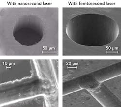
FIGURE 10 shows some experimental results regarding glass processing with a 266 nm (UV) ns laser and with a 780 nm (IR) 100 fs laser, respectively. In this case, the femtosecond laser photos on the right side represent a >2 million times shorter pulse duration. This, in turn, creates much cleaner and smoother hole features.
Ultrafast laser usage
As shown above, femtosecond lasers can be used for microprocessing many types of materials: metals, polymers, semiconductors, ultrahard materials, transparent materials, tissues, etc. However, the properties of materials, especially optical and thermal properties, require selection of proper laser parameters and laser ablation thresholds.
Typically, metals have very short laser penetration depth (tens of nm) and strong optical absorption — hence the laser ablation threshold is relatively low compared to transparent materials. In contrast, wide-bandgap materials require high laser-pulse intensities for generating seed-free electrons and for reaching the multiphoton impact avalanche ionization processes.5 Therefore, the laser ablation threshold for wide-bandgap materials is also relatively higher. Some wide-bandgap materials include diamond, silicon carbide (SiC), aluminum nitride (AlN), gallium nitride (GaN), and boron nitride (BN).
Compared to micromachining with CW and long-pulse lasers, ultrafast lasers have several advantages: micro-sized structure creation, no collateral damage to the surroundings, clean process look, small HAZ creation, no material property change, and capability for transparent material sub-surface engraving. Femtosecond laser micromachining is a rapidly advancing area of ultrafast laser applications. Because the machining process is not dependent on linear absorption at the laser wavelength, virtually any dielectric, metal, or mechanically hard material can be machined by the same laser beam. Femtosecond laser micromachining will find many more applications in the near future, including:
- Sub-micron material processing: Material milling, hole drilling, grid cutting
- Surface structuring: Photolithographic mask repair, surface removal or smoothing without imparting any thermal influence into the underneath sub-layers or the substrate
- Photonics devices: Machining of optical waveguides in bulk glasses or silica, and inscription of grating structure in fibers
- Biomedical devices: Use of femtosecond lasers for stent manufacture or eye surgery
- Microfluidics: Microfluidic channels and devices
- Displays and solar: Thin-film ablation, solar cell edge isolation, P1-P3 processing
Summary
Ultrafast laser micromachining is an emerging technology for high-precision and cold-ablation material microprocessing. Although many superior applications of ultrafast laser micromachining have been found over conventional laser processing, its advantages and potential uses need to be further explored.
This article has provided a back-to-basics description of ultrafast laser microprocessing- from laser sources and basic mechanisms, to potential applications. As the world continues to move toward a nanoscale technology era, micro-scale processing will become a valuable tool for technology development in the future. Certainly, ultrafast lasers and ultrafast laser micromachining will find many more applications in both the scientific and industrial markets. ✺
Lonnie Lucas Ph.D ([email protected]) and Jim Zhang Ph.D are with Applied Energetics in Tucson, Arizona.
References
[1] M. Peach, “Laser 2011: Ultrafast lasers hit the factory floor,” Optics.org, May 23, 2001.
[2] M.D. Perry, B.C. Stuart, P.S. Banks, M.D. Feit, V. Yanovsky, & A.M. Rubenchik, “Ultrashort-pulse laser machining of dielectric materials,” J. of Appl. Phys. 85, 9, 6803-6810 (1999)
[3] J. Bonse, S. Baudach, J. Krüger and W. Kautek, “Femtosecond laser micromachining of technical materials,” SPIE Proceedings vol. 4065, pp. 161-172 (2000)
[4] W. Kautek and J. Krüger, “Femtosecond-pulse laser ablation of metallic, semiconducting, ceramic, and biological materials, SPIE Proceedings vol. 2207, pp. 600-611 (1994)
[5] M. Meunier, B. Fisette, A. Houle, A.V. Kabashin, S.V. Broude, and P. Miller, “Processing of metals and semiconductors by a femtosecond laser-based microfabrication system,” SPIE Proceedings vol. 4978, 169-179 (2003)
[6] L. Jiang and H. L. Tsai, “Femtosecond Lasers Ablation: Challenges and Opportunities,” NSF workshop on “Unsolved Problems and Research Needs in Thermal Aspects of Material Removal Processes,” June 10-12, Stillwater, OK (2003).
[7] Product introduction on www.appliedenergetics.com.
[8] D.J. Richardson, J. Nilsson, and W.A. Clarkson, “High-power fiber lasers: Current status and future perspectives” [Invited], J. Opt. Soc. Am. B, vol. 27, B63 (2010)
[9] Product introduction on www.calmarlaser.com
[10] M.R.H. Knowles, “Micromachining of transparent materials with nano-, pito-, and femtosecond lasers: A review” AILU Workshop: Industrial and research opportunities in laser micro and nano processing, Daresbury Laboratory, Warrington, UK. Available on knowledgebase of www.oxfordlasers.com.
Editor’s Note: With the rapid growth of ultrafast-pulse laser processing in industrial applications, ILS decided that a back-to-basics feature was warranted for those new to this technology, and for those in need of a refresher. Lonnie Lucas and Jim Zhang accepted the challenge. This primer on the subject, written for laymen, is a neat, succinct summary of the technology.
Glossary
ablation craters: The surface denting structure ablated by laser pulses
ablation rate: Material volume removal speed by laser or laser pulses
ablation threshold: The minimum laser pulse fluence (J/cm2) for starting the ablation of material
binding energy of atom: The energy required to disassemble an atom into free electrons and a nucleus
electron-phonon coupling time: Time for Intermolecular vibrations (or phonons) and electron-phonon coupling to occur
electron-to-lattice energy transfer time: The time period required for electrons to transfer their kinetic energy to the crystal lattice, a few picoseconds period indicated by studies
heat-affected-zone (HAZ): The area of base material, either a metal or a thermoplastic, which has had its microstructure and properties altered by laser ablation or heat intensive cutting operations
wide-bandgap materials: Having large energy difference (e.g, >5 eV) between the top of the valence band and the bottom of the conduction band for the material
incubation effect: For laser ablation process, it indicates the thermal influence contribution of the previous laser pulses to the ablation induced by the following pulses
inverse Bremsstrahlung: One of the important mechanisms for heating plasmas with lasers in the intense fields required for laser fusion
ionization process: The physical process of converting an atom or molecule into an ion by adding or removing charged particles such as electrons or other ions
laser fluence: The total pulse energy over the area under 1/e2 laser beam profile, typically in a unit of J/cm2
laser pulse overlap: In laser process scan, the beam area overlap ratio between two consecutive laser pulses
laser repetition rate: The frequency of laser pulses (i.e., 1/pulse-to-pulse separation period)
material evaporation: The material is evaporated by a heating source into a vapor phase
material removal rate (5 µm3/µJ): Volume of material removal per certain pulse energy
micromachining: Creating microstructures either in bulk or on surface of materials, by deposition and ablation of different structural layers
multiphoton absorption: The excitation of an atom or other microscopic system to a higher quantum state by simultaneous absorption of two or more photons, which together provide the necessary energy
multiphoton ionization threshold: The minimum laser power density for creating at least a two-photon ionization process
plasma plume: Plasma “cloud” generated by high intensity laser pulses and composed of cluster of electrons, ions, and target material particles above the surface of the sample
plasma shielding effect: At high fluence, the laser pulse induced plasma efficiently attenuates the incoming laser radiation (plasma shielding) and reduces the ablation rate
pulse duration: Time period at full width of half maximum of pulse temporal profile
self-focusing threshold: A minimum laser intensity for having a non-linear optical process induced by the change in refractive index of materials exposed to intense electromagnetic radiation
squared crater diameter (D2): The diameter squared of the laser ablation area, D2 = 2ωo2ln(F0/Fth), which is usually used for experimentally determining laser material ablation threshold, where ωo is the 1/e2 beam radius of the Gaussian beam on the sample, F0 and Fth are laser pulse peak fluence and ablation fluence threshold
thermal conductivity: In physics, thermal conductivity is the property of a material’s ability to conduct heat
More Industrial Laser Solutions Current Issue Articles
More Industrial Laser Solutions Archives Issue Articles
