Micro-production of the future requires systems that can provide prototypes, one-off production, and small series quickly and efficiently. This includes highly flexible, intelligent, and high-precision production systems, and the demand for these solutions is driven by the steady trend toward miniaturization in many application areas.
Examples of this are in medicine, environmental protection, and the process engineering industry, all of which need small, reliable test systems that work as quickly and accurately as lab-on-a-chip. Such systems require precise manipulation and control of very small amounts of liquid. Microfluidic channels are required to safely move small volumes, with functioning components such as filters, stirrers, etc. in them. Previous production methods limited the freedom of design for such microfluidic channels. To produce functional substructures within these was virtually impossible. With the help of innovative additive-microfabrication technology, these barriers can now be overcome without compromising quality or precision.
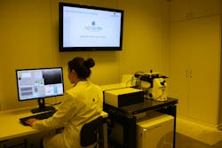
Another area that requires high-precision structures is photonics. With light, many times the amount of data can be transferred when compared to conventional microelectronics. To exploit this advantage in the communication between optoelectronic components, high-performance optical cable connections (chip-to-chip interconnects) can be printed with the high-resolution Photonic Professional GT systems from Nanoscribe (FIGURE 1). Micrometer-small, three-dimensional (3D) polymeric optical waveguides, called photonic wire bonds (PWBs), are produced directly on silicon-based components. According to the respective requirements, optimally adapted optical interfaces can be generated that form the basis of optical multi-chip modules. This new technology allows for the development of unprecedented high transfer rates of more than 5Tbit/s, which is an important milestone for both telecommunications and consumer electronics.
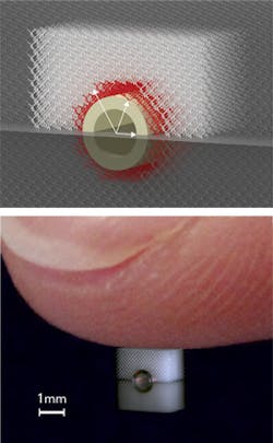
Micro-electromechanical systems (MEMS) identifies a field of miniaturized systems tailored to one another, consisting of sensors, actuators, and microstructures. For applications in microrobotics, specific microstructures, for instance, are inserted into aqueous media, making it possible to grip these with optical tweezers and move them. This feature relies on the fact that heavily focused light exerts force on microscopic objects and that these are drawn to the focused light beam. Thus, such micro-optical objects can be freely moved as a kind of optically stimulated microrobot in 3D space.Maskless lithography
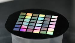
Without the additional cost of purchasing further equipment, the Photonic Professional GT system can also be used for maskless lithography in simple workflows. This allows the direct printing of diffractive optical elements, high-resolution grating structures, or individual diffractive dot patterns (e.g., QR codes) in a single step and with extreme precision (FIGURE 4). The parts can be used as security features in product protection applications (FIGURE 5), as the economic damage caused by plagiarizing of merchandise is in the billions. Conventionally, production of these labels is carried out by various methods that usually need a mask for production. This means that there is also lots of future potential in the technology of maskless lithography.Driving accuracy to the top
Nanoscribe devices operate on the basis of two-photon polymerization (TPP) with photosensitive materials as the starting material. Here, the liquid resist is locally solidified by a photochemically triggered polymerization. The system uses laser light in the near-infrared with a wavelength of 780nm, to which the photoresist is transparent. The laser is femtosecond-pulsed, with a repetition rate of 80MHz. The absorption of two photons triggers the polymerization exclusively in the focus and not along the beam path. Unexposed material is easily washed out at the end. The resolution of this true 3D rapid prototyping process is better than 500nm and delivers complex, self-supporting microstructures.
This method also allows an extremely high degree of flexibility because the computer-controlled beam guidance can transfer 3D CAD models directly into 3D structures of any complexity. Furthermore, this has the great advantage that production costs and component complexity are largely decoupled.
The size of the focal spot and, thus, the polymerized volume per laser pulse—called voxel (pixels + volume)—can be controlled via the numerical aperture (NA) of a lens and the laser power. A focusing lens with high NA will have a very small voxel and one can create structures with extreme resolution. There are two strategies to safely move the voxel through the sample. With a fixed-beam moving sample (FBMS), high-precision positioning units move the substrates relative to the focal point on very precise trajectories. Arbitrarily shaped complex structures with finest lateral structure sizes in the submicron range are possible through this approach. The moving-beam fixed sample (MBFS) solution enables much faster production speeds with a layered construction process. Precise coordination of beam deflection, sample movement, and modulation of the laser intensity are prerequisite.
Optimizing the size of structures
To create mesoscale structures, the dip-in laser lithography (DiLL) method invented by Nanoscribe is a proven technology and especially useful in 3D printing. This provides the means of high-resolution 3D structures far beyond the working distance of the lens, guaranteeing constant quality over the entire print height—that is, the figure quality is independent of the print height. To get the best results, the lens is immersed in the liquid photoresist, acting as an immersion medium.
Immersion lithography allows for a sharper picture in photolithographic patterning. An immersion liquid with a refractive index as high as possible replaces the air in the gap between the last lens and the wafer surface. This allows, in comparison with similar systems without immersion medium, the production of smaller structures since a larger NA and depth of focus are achieved.
This depth of focus detemines the range—in the direction of the optical axis of the illumination system—within which the focus for a sharp image is sufficient. Since an optimal exposure throughout the thickness of the photoresist layer is desired, the depth of focus must therefore be sufficiently large. Similar to the resolving power, the focal depth depends on the wavelength used, the applied NA, and the immersion medium. The major advantage is that DiLL is no longer limited by the working distance of the lens. Thus, structures can be printed measuring up to the millimeter range (FIGURE 6).Printing at the highest speed
To achieve high performance, a precise galvo scanner can deflect the laser focus, together with a stage for ultraprecise movements in space. With a writing speed of 10mm/s, the galvo technology accelerates the layer printing in two orders of magnitude, which melts manufacturing minutes to seconds. To write larger areas, adjacent polymerized volumes must be combined intelligently.
Almost can't go smaller
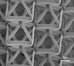
If conventional methods are reaching their limits such as stereolithography at layer thicknesses of 50–150μm, then there is no alternative to 3D laser lithography. The resolution is, in comparison to stereolithography, about 10–100X as high. Structural details of 1μm and less are standard, while surfaces are optically smooth. This high resolution is demanded and used in structures with heights from several hundred nanometers up to the millimeter range.
Another possibility to create micro components with additive laser writing is micro-stereolithography (micro SLA). In micro SLA, the object to be produced is dipped into the resist and a focused laser beam writes the corresponding structures. After one round, the part is lowered, new resist is distributed on it, and the laser starts again. The polymerization is initiated by a single photon. This solidification takes place over the entire resist thickness along the laser beam. The polymerized volume is significantly larger than that of TPP. Therefore, the thicknesses of the individual layers are at least 10μm. With TPP, however, distances of 100nm—at best—are created.
Theoretically, even slightly smaller structures are possible with TPP, but industry demands tend more toward higher writing speeds and component sizes of less than 1cm at maximum complexity.
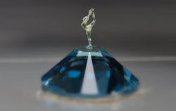
Nanoscribe now meets these demands by offering a new lens with a larger scan area. With DiLL, structures up to 4mm high are possible. For these demands, a specially developed resist polymerizes at lower laser power, thus working quickly and providing optically smooth surfaces.The new software has been optimized for high writing speed. Bigger structures require larger amounts of data. For this purpose, new writing strategies for the guiding of the laser beam are necessary. This makes the system faster by a factor of about 10, allowing a delicate dancer figurine to be finished in less than one hour (FIGURE 7).
